
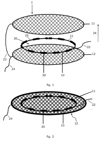
A device for generating plasma (1) comprises a high voltage electrode (10) as well as at least one external electrode (11, 12), wherein the high voltage electrode (10) at least in one coordinate direction (34) is arranged between conductive material of at least one external electrode (11, 12). The high voltage electrode (10) is covered with a dielectric (21) at least one side facing an external electrode (11, 12). Between the respective external electrode (11, 12) and the high voltage electrode (10) over its longitudinal extension at least one spacer element (20) is present, which at least in the region of its arrangement electrically insulates the respective external electrode (11,12) from the high voltage electrode (10) and which positions the respective external electrode (11, 12) at a constant distance from the high voltage electrode (10), wherein the spacer element is a gas-permeable foil.
Figures 1 and 2 of the Patent Specification
EP3171676 B1
1. A plasma generating device (1) comprising a high-voltage electrode (10) as well as at least one external electrode (11, 12), wherein the high-voltage electrode (10) is, at least in one coordinate direction (34), arranged between conductive material of at least one external electrode (11, 12) and the high-voltage electrode (10) is covered with a dielectric (21) at least on one side facing an external electrode (11, 12) of the plasma generating device (1), and wherein between the respective external electrode (11, 12) and the high-voltage electrode (10) over its longitudinal extension at least one spacer element (20) is present, which at least in the region of its arrangement electrically insulates the respective external electrode (11, 12) from the high-voltage electrode (10) and which positions the respective external electrode (11, 12) at a constant distance from the high-voltage electrode (10), characterized in that the spacer element (20) is planar in design, and the spacer element (20) is a perforated and/or structured, gas-permeable foil made of an electrically non-conductive elastomer.
| Field | Value | |||||||||||||||
|---|---|---|---|---|---|---|---|---|---|---|---|---|---|---|---|---|
| Patent Family |
| |||||||||||||||
| Applicant(s) | ||||||||||||||||
| Inventors |
| Field | Value |
|---|---|
| Plasma Source Name | |
| Plasma Source Application | |
| Plasma Source Specification |